Последний блог
Дает ли рынок печатных плат импульс роста лазерным компаниям? Каковы преимущества мощных наносекундных УФ-лазеров?
Jul 28 , 2022Does the PCB market bring growth momentum to laser companies? What are the advantages of high power nanosecond UV lasers?
In 2019, the growth rate of the laser processing market has further slowed down. The maturity of some application markets and the competition in the Red Sea have also caused related companies to face the dilemma of increased operating pressure and declining performance. The new crown pneumonia epidemic in 2020 has given the development of laser companies. overshadowed. In such an environment, OFweek Laser Network found that the laser market related to PCB processing is still growing. In the data disclosed by some listed companies, PCB business orders have become the main driving force supporting performance growth. How is the development of the PCB market? And why can it bring huge growth momentum to laser companies?
Rapid development of PCB and FPC industry, huge market increment
PCB is the abbreviation of Printed Circuit Board. It is one of the important components of the electronics industry and is used in almost all electronic products. Its main function is to realize the electrical interconnection between various components. The PCB consists of an insulating base plate, connecting wires and pads for assembling and soldering electronic components, and has the dual functions of a conductive circuit and an insulating base plate. Its manufacturing quality can directly affect the reliability of electronic products. It is the basic industry of today's electronic information product manufacturing, and it is also the industry with the largest output value in the current global electronic component subdivision industry.
uv laser | green laser | Ultraviolet lasers | uv dpss laser | nanosecond laser | UV laser source | Solid State Lasers
The application market of PCB is very wide, including consumer electronics, automotive electronics, communications, medical, military, aerospace and so on. At present, the rapid development of consumer electronics and automotive electronics has become the main field of PCB applications. For a long time, the global PCB output value was mainly concentrated in North America, Europe and Japan. After 2000, the focus of the PCB industry began to shift to the Asian region, especially the Chinese market. In 2009, the output value of the PCB industry in mainland China accounted for about 1/3 of the world's total. By 2017, it had reached 50.5%, accounting for half of the global PCB output value.
Data source: Prismark, OFweek Industrial Research Institute
In 2019, affected by trade frictions, declining terminal demand and exchange rate depreciation, the global PCB output value declined slightly, but the Chinese market benefited from the rapid development of 5G, big data, cloud computing, artificial intelligence, Internet of Things and other industries, becoming the only one in 2019. growing area. According to Prismark data, the size of China's PCB market in 2019 was about US$32.9 billion, accounting for 53.7% of the world.
In the PCB application of consumer electronics, FPC develops the fastest, and its proportion in the PCB market continues to increase. FPC is the abbreviation of Flexible Printed Circuit, which is a highly reliable and reliable product made of polyimide (PI, also known as PI cover film in the industry) or polyester film as the base material. It is an excellent flexible printed circuit board with the characteristics of high wiring density, light weight, thin thickness and good bendability. Under the current trend of intelligent, light and thin mobile electronic products, FPC is widely used due to its advantages of high density, light weight, thin thickness, bending resistance, flexible structure, high temperature resistance, etc. the only solution.
The rapidly developing PCB market has fostered a huge derivative market. With the development of laser technology, laser processing has gradually replaced the traditional die-cutting process and has become an important part of the PCB industry chain. Therefore, in the context of the slowdown in the overall growth rate of the laser market, the PCB-related business can still maintain high growth.
The advantages of laser in PCB and FPC processing
The application of laser on PCB mainly includes cutting, drilling, marking, etc., especially cutting. Compared with the traditional die-cutting process, laser cutting is a non-contact process, without the need for expensive molds, and the production cost is greatly reduced; in addition, the traditional process is difficult to solve a series of problems such as burrs, dust, stress, and inability to process curves on the edge. The laser spot is only ten microns after focusing, which can meet the processing requirements of high-precision cutting and drilling, and solve a series of problems left in the traditional process. This advantage is catering to the development trend of precision circuit design, and it is an ideal tool for PCB, FPC, PI film cutting.
Фактически, применение технологии лазерной резки печатных плат в производстве печатных плат началось раньше, но на ранней стадии использовалась лазерная резка CO2, которая имеет большое тепловое воздействие и низкую эффективность и не смогла добиться хорошего развития. Он используется только в некоторых специальных областях (таких как научные исследования, военные и т. д.). С развитием лазерных технологий в производстве печатных плат можно использовать все больше и больше источников света, и был обнаружен прорыв в промышленном применении лазерной резки печатных плат.
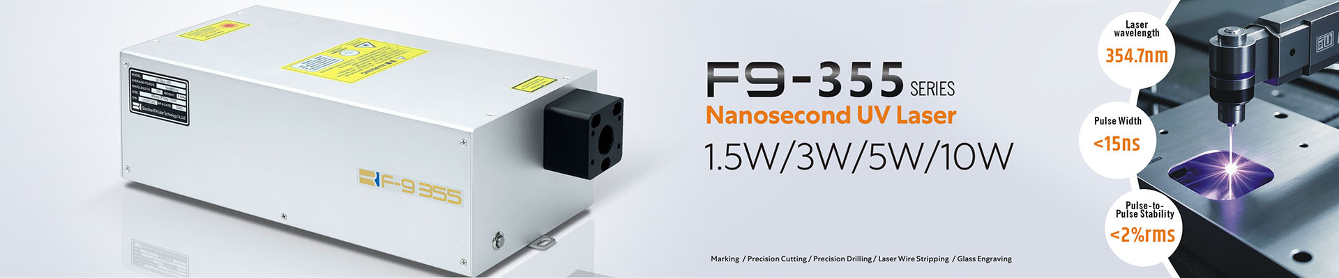
В настоящее время лазеры, используемые для резки пленок FPC и PI, в основном представляют собой наносекундные твердотельные УФ-лазеры, а длина волны обычно составляет 355 нм. По сравнению с инфракрасным излучением с длиной волны 1064 нм и зеленым светом с длиной волны 532 нм, УФ-излучение с длиной волны 355 нм имеет более высокую энергию одиночных фотонов, более высокую скорость поглощения материала, меньшее тепловое воздействие и более высокую точность обработки.
С принципиальной точки зрения, импульсная лазерная резка материалов может быть разделена на две ситуации: первая — это фотохимический принцип, использующий энергию одиночного фотона лазера для достижения или превышения энергии химической связи материала для разрыва некоторых химических связей материала. материал для резки; другой - свет. Согласно физическому принципу, когда энергия одиночного фотона лазера ниже, чем энергия химической связи материала, очень высокая плотность энергии в сфокусированном пятне превышает порог газификации материала, тем самым мгновенно газифицируя материал. и осуществление резки материала. Но на самом деле при резке пленки FPC или PI с помощью УФ-лазера принципы фотохимической и фотофизической резки существуют одновременно.
Следующие два принципа обработки объясняются на примере пленки PI. Энергия связи связи CC и связи CN в нормальном состоянии составляет 3,45 эВ и 3,17 эВ соответственно, в то время как энергия одного фотона УФ-лазера с длиной волны 355 нм составляет 3,49 эВ, что выше, чем у связи CC и связи CN в нормальном состоянии. непосредственно разрушают химические связи материалов. (Ссылка: Zhang Fei, Duan Jun, Zeng Xiaoyan и др. Исследование обработки глухих переходных отверстий в гибких печатных платах ультрафиолетовым лазером с длиной волны 355 нм [J]. China Laser, 2009, 36(12):3143-3148.)
При фотофизическом эффекте будет происходить выделение и накопление тепла, а температура материала будет продолжать расти. Когда температура материала PI выше 600 ° C, соотношение элементов N и O будет продолжать уменьшаться по сравнению с элементом C, и в конечном материале в основном преобладает элемент C, то есть материал карбонизируется. . Формула диффузионного расстояния L=[4Dt]^1/2, где D — коэффициент температуропроводности материала, t — ширина лазерного импульса. (Ссылка: Zhang Peng, Chi Weidong, Shen Zengmin. Влияние высокотемпературной карбонизации на структуру и свойства тонких пленок полиимида (PI) [J]. Carbon Technology, 2008, 27(6):10-12.)
Можно видеть, что, когда материал является постоянным, чем больше ширина лазерного импульса, тем больше расстояние диффузии тепловой энергии, генерируемой лазером на материале, и тем больше термическое повреждение материала. Следовательно, чем уже ширина импульса, тем лучше эффект обработки.
Наносекундный УФ-лазер мощностью 20 Вт/25 Вт: более высокая мощность, лучший эффект
Как упоминалось выше, индустрия печатных плат в моей стране выиграла от быстрого развития новых отраслей, таких как 5G и большие данные. Появление новых отраслей и новых технологий также выдвинуло более высокие требования к отраслям резки пленки FPC и PI. Чтобы добиться меньшей карбонизации и более высокой эффективности, лазерные компании также постоянно внедряют технологические инновации и постоянно изучают более высокие частоты, более узкую ширину импульса и более высокую мощность.