Последний блог
Лазерная депанелизация печатных плат с использованием мощного УФ-лазера с длиной волны 355 нм
Feb 06 , 2023PCB Laser Depanelizing Using a high power UV Laser source
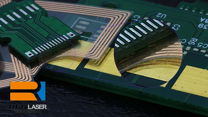
One of the methods gaining in popularity for singulating rigid/flex, rigid and flex circuit
boards post assembly is through the use of laser routing. This method has the
advantage of speed, positional accuracy, no tooling wear and lastly no induced
mechanical stresses on components during the singulating process.
There are several cases where laser routing of printed circuit boards is desirable:
o when a high degree of precision of the final assembly is required (think
“tight fit” of a board in to an assembly) or
o when numerous materials need to be cut through and the number and
type of depanelizing steps is to be limited (think “not compromising
cutting one material by using a technique that does not work well on a
second or third material”) or when
o unusual board shapes come up in a design or finally when
o highly sensitive components are placed near the cut out lines of the PCB
need to be treated gingerly.
There are a variety of depaneling options available for PCBs, each with its
own set of advantages and disadvantages.
PCB Depaneling Options
The methods for straight line PCB singulating, which are set up for rectangular-shaped
PCBs, all cut or crush the edge of the board edge. These methods include die cutting,
punching or V-scoring the assembly or by using a wheel cutter or a saw.
The sawing method typically uses a single rotating blade spinning at high RPM to cut
the panel into the shapes required. This method produces heat in the cut out area as
well as creating debris as a byproduct of the cutting operation.
In V-scoring the depth of the thickness of the board is 30-40% of the original board
thickness as it is cut from both sides of the board. After assembly the board is broken
at this v-score line. Alternately a “pizza cutter” cuts through the V-score of the panel
and cuts the remaining web until the boards are in their final cutout shape thereby
putting strain on the components and solder joints-especially those near the board
edge.
In another method, the singulated board outline can be punched out form the panel.
This requires that a new punch be used for every single type of circuit board which
means it is not a flexible method of board cut out. The punch force can also bend or
deform the edges of the PCB. Sharp edges of a well-maintained die must be the norm
in order to get a defect-free cutout.
In board routing and subsequent “nibbling” on a board outline can also be
cut out. Boards are routed prior to assembly. The remaining attached
points are drilled with a small drill thereby making it easier to break
the boards out from the panel post board assembly. This leaves socalled “mouse bite” patterns behind. The routing takes up panel space
as there are keep out requirements around the edge of the board cut
out area. The routing can also reduce panel stiffness which is typically
required and desire during the initial stages of the PCB assembly
process. The advantage the routing process is that curved and nonlinear line patterns can be cut using the router bit.
In each of the above techniques, all of which are mechanical in nature, the board
edges, parts near the cut out area as well as the solder joints will have a high degree of
stress placed on them during the cutting process. This stress may cause delamination of
the board near its edges or develop space in and round the glass fibers near the board
edge. Both of these anomalies may lead to moisture ingress in to the board which may
lead to reliability problems down the road. These potential problems enlarge the “keep
out” areas of the components along the periphery of the boards.
Laser Machining Options
There are several methods by which laser machining can be used to create the board
cutout patterns including perforations, hold-in tabs and scoring. The precision of the
laser cutting source allows for much smaller PCB geometries to be singulated. The
precision of the laser is quite tight especially when compared to other mechanical
methods. The C02 laser sources are positionally and dimensionally within 2 mils (50um)
while the UV sources are within 1 mil (25 um)
Perforations
Similar to scoring or v-grooves, laser perforations are another option for tool-less PCB
removal from a panel. Perforations can be laser formed to any size and spacing to meet
the desired removal and securement forces.
Hold-in Tabs
Hold-in tabs are small uncut sections around the board used to secure the board in the
panel. The hold-in tabs are used due to the ease of handling small parts or part
securement for additional processing. The hold-in tab width is chosen based on the
amount of force desired to remove the individual board from the panel/sheet or known
forces to be applied by downstream processes like component loading or electropolishing. The laser can create tabs in most any material and to any width and location
about the board.
Scoring
Laser scoring produces a limited depth ablation line in the board material or materials.
The depth is generally 50% of the material thickness but can be controlled to a desired
depth. The scoring acts similar to the hold-tab to secure the PCB in to the panel, but
позволяет «вырезать» отдельные детали. Лазерные линии подсчета также могут использоваться в качестве
преднамеренный путь для снятия напряжения или распространения трещины.
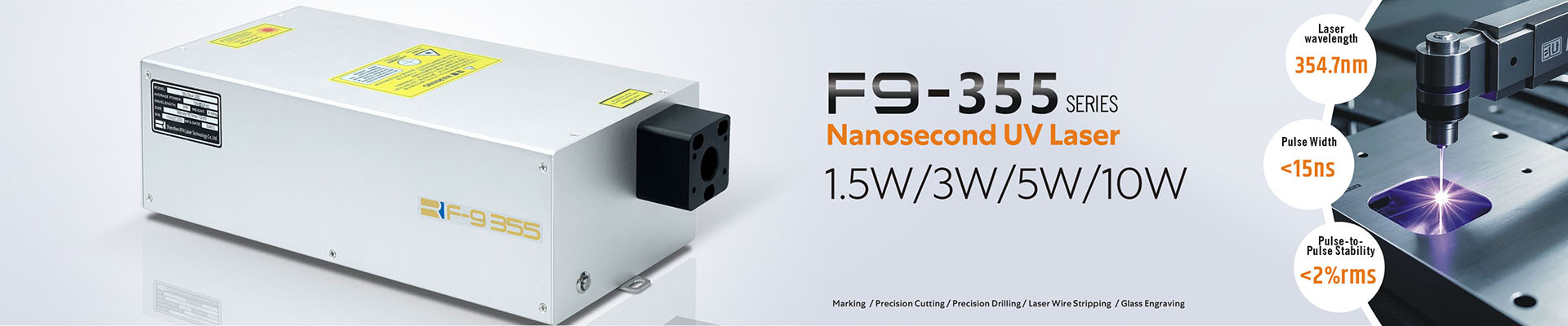
Как работают УФ-лазеры с длиной волны 355 нм
УФ-лазеры, работающие на длине волны 355 нм, используются для абляции или разрушения материала платы. А
высокоэнергетический лазерный импульс испаряет и удаляет верхний слой, превращая его в
микрочастицы пыли. Для этого необходимо, чтобы материал, будь то ФР-4, полиимид,
металлы или их комбинация должны быть в состоянии поглощать импульс. Лазер
луч проходит вперед и назад по месту разреза, удаляя понемногу за раз.
Это означает, что, поскольку за один раз испаряется лишь небольшое количество материала,
локальный эффект нагрева сведен к минимуму. На самом деле, измерения, проведенные вблизи зоны резки
(в пределах 1,5 мм от области реза) показывают, что повышение температуры значительно ниже 1000°C ниже, чем для профиля оплавления (1). В то время как другие лазеры с более короткой длиной волны могут быть более
оптимальны с точки зрения производительности, их использование ограничено высокими требованиями к капиталу
Чтобы сократить время резки и связанные с этим расходы, лазерный луч
управляемый» с помощью гальванометра (гальво). Это отслеживает траекторию резки в материале по
небольшая площадь. Этот подход к сканеру заставляет луч перемещаться с очень высокой скоростью.
скорости в одном и том же месте на небольшой площади. Эта скорость находится в диапазоне от 100 до
1000 мм/сек. Это гарантирует, что луч находится в одной и той же области только в течение короткого периода времени.
времени, тем самым сводя к минимуму влияние локального нагрева.
Реперные точки на доске могут помочь определить относительное требуемое расположение луча.
место резки. Прецизионный стол XY используется для больших механических перемещений и
корректировки, в то время как гальво берет на себя микродвижения и корректировки
расположение.
Заключение
Лазерное разделение печатных плат имеет свою нишу применения там, где платы расположены на небольшом расстоянии друг от друга,
где критически важны геометрические допуски и где линии расположения вырезов очень
близко к компонентам. Способ позволяет производить точный раскрой досок во время
процесс разделения с очень небольшим нагревом доски и очень небольшим механическим напряжением
по сравнению с традиционными методами разделения панелей.